- 您现在的位置:买卖IC网 > Sheet目录2006 > LTC2305CDE#TRPBF (Linear Technology)IC ADC 12-BIT 2CHN 12-DFN
LTC2301/LTC2305
21
23015fb
separated as much as possible. Care should be taken not
to run any digital signals alongside an analog signal. All
analog inputs should be shielded by GND. VREF, REFCOMP
and VDD should be bypassed to the ground plane as close
to the pin as possible. Maintaining a low impedance path
APPLICATIONS INFORMATION
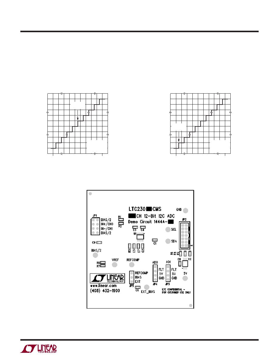
Figure 15a. Top Silkscreen
for the common return of these bypass capacitors is es-
sential to the low noise operation of the ADC. These traces
should be as wide as possible. See Figures 15a–15e for
a suggested layout.
Figure 13. Bipolar Transfer Characteristics (2’s Complement)
Figure 14. Unipolar Transfer Characteristics (Straight Binary)
INPUT VOLTAGE (V)
0V
OUTPUT
CODE
(TWO’S
COMPLEMENT)
–1
LSB
23015 F13
011...111
011...110
000...001
000...000
100...000
100...001
111...110
1
LSB
BIPOLAR
ZERO
111...111
FS/2 – 1LSB
–FS/2
FS = 4.096V
1LSB = FS/2n
1LSB = 1mV
INPUT VOLTAGE (V)
OUTPUT
CODE
23015 F14
111...111
111...110
100...001
100...000
000...000
000...001
011...110
011...111
FS – 1LSB
0V
UNIPOLAR
ZERO
FS = 4.096V
1LSB = FS/2n
1LSB = 1mV
发布紧急采购,3分钟左右您将得到回复。
相关PDF资料
LTC2306CDD#PBF
IC ADC 12BIT 2CH 500KSPS 10-DFN
LTC2351HUH-12#TRPBF
IC ADC 12BIT 1.5MSPS 32-QFN
LTC2351HUH-14#TRPBF
IC ADC 14BIT 1.5MSPS 32-QFN
LTC2355IMSE-14#TRPBF
IC ADC 14BIT 3.5MSPS 10-MSOP
LTC2356IMSE-14#TRPBF
IC ADC 14BIT 3.5MSPS 10-MSOP
LTC2366HTS8#TRPBF
IC ADC 12BIT 3MSPS TSOT23-8
LTC2379HMS-18#PBF
IC ADC 18BIT SPI/SRL 16MSOP
LTC2380HMS-16#TRPBF
IC ADC 16BIT 2MSPS 16-MSOP
相关代理商/技术参数
LTC2305CMS#PBF
功能描述:IC ADC 12-BIT 2CHN 12-MSOP RoHS:是 类别:集成电路 (IC) >> 数据采集 - 模数转换器 系列:- 标准包装:2,500 系列:- 位数:16 采样率(每秒):15 数据接口:MICROWIRE?,串行,SPI? 转换器数目:1 功率耗散(最大):480µW 电压电源:单电源 工作温度:-40°C ~ 85°C 安装类型:表面贴装 封装/外壳:38-WFQFN 裸露焊盘 供应商设备封装:38-QFN(5x7) 包装:带卷 (TR) 输入数目和类型:16 个单端,双极;8 个差分,双极 配用:DC1011A-C-ND - BOARD DELTA SIGMA ADC LTC2494
LTC2305CMS#PBF
制造商:Linear Technology 功能描述:ADC, 12BIT, 14KSPS, MSOP-12
LTC2305CMS#TRPBF
功能描述:IC ADC 12-BIT 2CHN 12-MSOP RoHS:是 类别:集成电路 (IC) >> 数据采集 - 模数转换器 系列:- 标准包装:2,500 系列:- 位数:16 采样率(每秒):15 数据接口:MICROWIRE?,串行,SPI? 转换器数目:1 功率耗散(最大):480µW 电压电源:单电源 工作温度:-40°C ~ 85°C 安装类型:表面贴装 封装/外壳:38-WFQFN 裸露焊盘 供应商设备封装:38-QFN(5x7) 包装:带卷 (TR) 输入数目和类型:16 个单端,双极;8 个差分,双极 配用:DC1011A-C-ND - BOARD DELTA SIGMA ADC LTC2494
LTC2305HMS#PBF
功能描述:IC ADC 12-BIT 2CHN 12-MSOP RoHS:是 类别:集成电路 (IC) >> 数据采集 - 模数转换器 系列:- 标准包装:2,500 系列:- 位数:16 采样率(每秒):15 数据接口:MICROWIRE?,串行,SPI? 转换器数目:1 功率耗散(最大):480µW 电压电源:单电源 工作温度:-40°C ~ 85°C 安装类型:表面贴装 封装/外壳:38-WFQFN 裸露焊盘 供应商设备封装:38-QFN(5x7) 包装:带卷 (TR) 输入数目和类型:16 个单端,双极;8 个差分,双极 配用:DC1011A-C-ND - BOARD DELTA SIGMA ADC LTC2494
LTC2305HMS#TRPBF
功能描述:IC ADC 12-BIT 2CHN 12-MSOP RoHS:是 类别:集成电路 (IC) >> 数据采集 - 模数转换器 系列:- 标准包装:2,500 系列:- 位数:16 采样率(每秒):15 数据接口:MICROWIRE?,串行,SPI? 转换器数目:1 功率耗散(最大):480µW 电压电源:单电源 工作温度:-40°C ~ 85°C 安装类型:表面贴装 封装/外壳:38-WFQFN 裸露焊盘 供应商设备封装:38-QFN(5x7) 包装:带卷 (TR) 输入数目和类型:16 个单端,双极;8 个差分,双极 配用:DC1011A-C-ND - BOARD DELTA SIGMA ADC LTC2494
LTC2305IDE#PBF
功能描述:IC ADC 12-BIT 2CHN 12-DFN RoHS:是 类别:集成电路 (IC) >> 数据采集 - 模数转换器 系列:- 标准包装:2,500 系列:- 位数:16 采样率(每秒):15 数据接口:MICROWIRE?,串行,SPI? 转换器数目:1 功率耗散(最大):480µW 电压电源:单电源 工作温度:-40°C ~ 85°C 安装类型:表面贴装 封装/外壳:38-WFQFN 裸露焊盘 供应商设备封装:38-QFN(5x7) 包装:带卷 (TR) 输入数目和类型:16 个单端,双极;8 个差分,双极 配用:DC1011A-C-ND - BOARD DELTA SIGMA ADC LTC2494
LTC2305IDE#TRPBF
功能描述:IC ADC 12-BIT 2CHN 12-DFN RoHS:是 类别:集成电路 (IC) >> 数据采集 - 模数转换器 系列:- 标准包装:2,500 系列:- 位数:16 采样率(每秒):15 数据接口:MICROWIRE?,串行,SPI? 转换器数目:1 功率耗散(最大):480µW 电压电源:单电源 工作温度:-40°C ~ 85°C 安装类型:表面贴装 封装/外壳:38-WFQFN 裸露焊盘 供应商设备封装:38-QFN(5x7) 包装:带卷 (TR) 输入数目和类型:16 个单端,双极;8 个差分,双极 配用:DC1011A-C-ND - BOARD DELTA SIGMA ADC LTC2494
LTC2305IMS#PBF
功能描述:IC ADC 12BIT I2C 12-MSOP RoHS:是 类别:集成电路 (IC) >> 数据采集 - 模数转换器 系列:- 标准包装:1 系列:microPOWER™ 位数:8 采样率(每秒):1M 数据接口:串行,SPI? 转换器数目:1 功率耗散(最大):- 电压电源:模拟和数字 工作温度:-40°C ~ 125°C 安装类型:表面贴装 封装/外壳:24-VFQFN 裸露焊盘 供应商设备封装:24-VQFN 裸露焊盘(4x4) 包装:Digi-Reel® 输入数目和类型:8 个单端,单极 产品目录页面:892 (CN2011-ZH PDF) 其它名称:296-25851-6